

Why Choose Our High-Performance TFT Small LCD Screens For Your Next Project?
Jul 15, 2025
Thin Film Transistor Liquid Crystal Display (TFT-LCD) represents the cutting-edge of active matrix display technology, where each liquid crystal pixel is individually driven by its own thin-film transistor. This revolutionary approach enables our small TFT LCD screens to deliver unparalleled image quality with high speed, brightness, and contrast ratios that outperform conventional display solutions
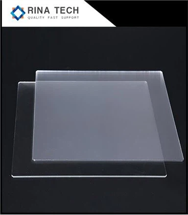
At the core of our TFT LCD technology lies a sophisticated architecture consisting of two parallel glass substrates sandwiching a liquid crystal layer. The lower substrate incorporates an array of precisely fabricated thin-film transistors (TFTs), while the upper substrate features a color filter system. When electrical currents pass through the TFT array, they generate controlled electric fields that manipulate the orientation of liquid crystal molecules. This molecular manipulation alters the polarization of light passing through, enabling precise control over each pixel's light transmission
Our manufacturing expertise allows us to produce TFT LCD screens ranging from compact 1-inch displays up to 10-inch panels, with resolutions tailored to meet diverse application requirements. The standard configuration includes:
Power board for AC/DC conversion (typically 220V/110V to 12V DC)
High-voltage board for backlight operation
Driver board (mainboard) with input interfaces (VGA/DVI/HDMI)
Key control board for user interface
The power system architecture demonstrates our engineering excellence, featuring:
Switching power supply converting AC mains to DC (12V/14V/18V/24V/28V options)
DC/DC converters generating multiple voltage rails (5V/3.3V/2.5V) for different subsystems
Flexible implementation options (external adapters or built-in power boards)
Our TFT LCD modules support various interface standards including SPI (4-6 wire), 8080 parallel (16-18 wire), and RGB interfaces, providing compatibility with different microcontroller architectures while optimizing for either pin count or refresh rate performance.
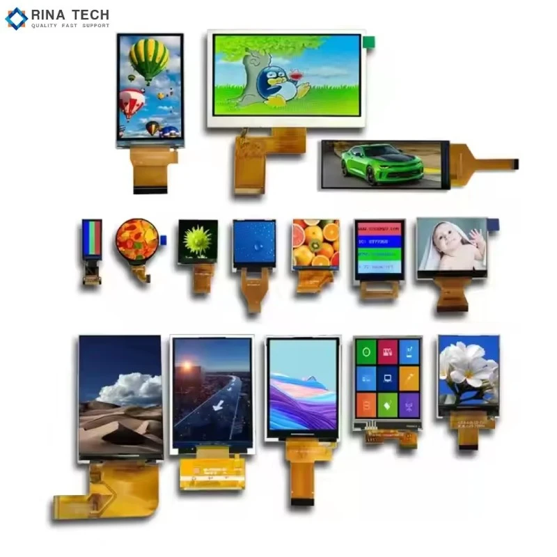
The exceptional performance of our TFT LCD screens stems from carefully selected materials and innovative construction techniques. The foundation begins with ultra-smooth, contamination-free glass substrates that undergo rigorous cleaning processes before any deposition begin. We employ several semiconductor technologies for the active layer, each offering distinct advantages:
Amorphous Silicon (a-Si): Our most cost-effective solution with 0.3-1 cm²/V.s electron mobility, ideal for standard resolution displays. The simple manufacturing process delivers high yields, particularly in larger panel sizes.
Indium Gallium Zinc Oxide (IGZO): With electron mobility of 10-25 cm²/V.s, this advanced material enables higher brightness, resolution (PPI), and refresh rates. IGZO-based displays are perfect for applications demanding superior performance.
Low-Temperature Poly-Silicon (LTPS): Our premium offering featuring >100 cm²/V.s mobility, supporting the most demanding specifications for brightness, resolution and refresh rates. Though more complex to manufacture, LTPS excels in compact, high-performance displays.
The transparent conductive layer utilizes Indium Tin Oxide (ITO), a critical component that combines excellent conductivity with high optical transparency (>90%). We deposit ITO through precision sputtering processes, creating the intricate electrode patterns that control liquid crystal alignment19.
Other essential materials in our display construction include:
Alignment layers: Polyimide films that orient liquid crystal molecules in predetermined directions
Color filters: Precisely patterned RGB elements with sub-pixel accuracy
Polarizers: High-performance films that control light polarization states
Liquid crystal mixtures: Custom formulations optimized for response time, viscosity, and temperature stability
Our manufacturing process incorporates specialized chemicals at each stage:
Photo-resists: High-resolution patterning materials for circuit formation
Etchants: Precision chemicals for defining thin film structures
Cleaners: Ultra-pure solutions maintaining process cleanliness
Sealants: Durable adhesives for panel encapsulation
The backlight system (for transmissive displays) combines LED light sources with advanced light guides and diffusers, engineered for uniform illumination and energy efficiency. We offer various brightness levels (typically 250-1000 cd/m²) to suit different ambient lighting conditions
Our small TFT LCD displays serve an expansive range of industries and applications, demonstrating remarkable versatility across multiple sectors:
Consumer Electronics
Smartphones and Tablets: High-resolution touch displays with excellent sunlight readability
Wearable Devices: Ultra-compact 1.5"-3.5" screens for smartwatches and fitness trackers
Portable Gaming: Fast-response panels for handheld gaming consoles
Digital Cameras: Bright, color-accurate preview screens
Industrial and Medical
Human-Machine Interfaces (HMI): Ruggedized displays for factory automation and control panels
Medical Monitoring: High-reliability screens for portable diagnostic equipment
Test and Measurement: Precision displays for oscilloscopes and analyzers
Kiosk Systems: Durable touchscreens for public information terminals
Automotive and Transportation
Instrument Clusters: Custom-shaped displays for vehicle dashboards
Center Stack Displays: Multimedia and navigation interfaces
Rear Seat Entertainment: Passenger viewing screens
Aircraft Displays: Aviation-grade panels with wide temperature tolerance
Emerging Technologies
IoT Devices: Low-power displays for smart home controllers
Augmented Reality: Compact panels for AR headset components
Robotics: Human-robot interaction interfaces
Drones: Lightweight FPV (First Person View) screens
Specific implementation examples showcase our technology's adaptability:
Industrial Control Panels: Our 2.4" TFT modules with resistive touch provide real-time parameter visualization (temperature, pressure) in harsh environments, paired with STM32 microcontrollers for robust operation
Smart Home Controllers: Energy-efficient 3.5" displays with capacitive touch enable intuitive control of thermostats, lighting, and security systems, featuring automatic brightness adjustment via ambient light sensors
Portable Medical Devices: Ultra-reliable 2.8" screens with wide viewing angles serve in glucose monitors and ECG devices, meeting stringent medical certification requirements14.
Automotive Rearview Systems: High-brightness 4.3" displays with wide dynamic range provide clear visibility in backup camera applications, even in direct sunlight
The education sector benefits from our displays in STEM projects, where Arduino and Raspberry Pi platforms utilize our SPI-interfaced modules for teaching GUI development and sensor data visualization14. Maker communities particularly appreciate our displays' compatibility with popular libraries like LVGL and emWin, accelerating project development.

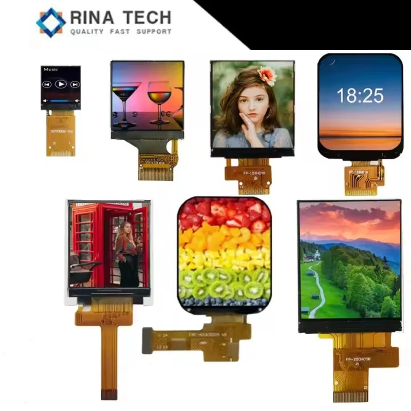
Our TFT LCD production follows an exacting three-stage manufacturing protocol that ensures consistent quality and performance:
Array Process (Front-End)
The foundation begins with pristine glass substrates undergoing meticulous cleaning. We then build the transistor array through a sophisticated sequence:
Gate Formation: Sputter-deposited metal layers (typically aluminum or copper alloys) are photolithographically patterned to create scan lines and gate electrodes. This involves:
Vacuum deposition of gate metal
Photoresist coating and UV exposure through precision masks
Wet etching to define circuit patterns
Insulator Deposition: Silicon nitride or oxide layers are applied via plasma-enhanced chemical vapor deposition (PECVD), creating the gate dielectric with thickness control within ±5%.
Active Layer Formation: Depending on technology (a-Si/IGZO/LTPS), the semiconductor layer is deposited and patterned, requiring precise control of composition and crystallinity.
Source/Drain Metallization: Another photolithography step forms the transistor contacts and data lines, completing the basic TFT structure
Passivation and ITO Patterning: Protective layers and transparent electrodes are added, with each step undergoing rigorous inspection via automated optical detection systems.
Cell Process (Mid-Stage)
This critical phase assembles the display core:
Alignment Layer Application: Polyimide coatings are applied to both TFT and color filter substrates, then mechanically rubbed to induce microscopic grooves for liquid crystal orientation
Spacer Dispersion: Precision micro-spheres (3-5μm diameter) are distributed to maintain exact cell gap uniformity.
Seal Printing: UV-curable epoxy is screen-printed on the perimeter, leaving an opening for later liquid crystal filling.
LC Injection: In a cleanroom environment, liquid crystal material is vacuum-injected through the seal opening, then permanently sealed
Module Assembly (Back-End)
The final integration stage:
Polarizer Lamination: Anti-glare and wide-viewing angle polarizing films are precisely aligned and bonded to the panel.
Driver IC Attachment: Using anisotropic conductive film (ACF), we bond flexible printed circuits (FPC) containing display drivers and controllers.
Backlight Integration: LED light guides and optical films are assembled behind the LCD panel (for transmissive designs).
Final Testing: Each module undergoes comprehensive electrical, optical, and reliability testing before shipment20.
Our quality assurance system implements:
Statistical Process Control (SPC) for real-time monitoring
Design and Process FMEA (Failure Mode Effects Analysis)
Strict RoHS and REACH compliance protocols
Full traceability from materials to finished goods
The entire manufacturing flow occurs in Class 1000 or better cleanrooms, with critical lithography steps performed in Class 100 environments. We maintain temperature and humidity control within ±0.5°C and ±3% RH to ensure process stability.
While specific packaging details weren't available in the search results, our extensive experience in display manufacturing ensures we employ industry-best practices for protecting delicate TFT LCD panels during shipping and handling. We understand that proper packaging is crucial for maintaining the integrity of these precision components throughout the supply chain.
For comprehensive packaging specifications and shipping standards tailored to your particular requirements, we recommend direct consultation with our technical sales team. They can provide detailed guidelines based on:
Your specific display model and size
Destination and transportation method
Environmental conditions during transit
Any special handling requirements
Our team stands ready to develop customized packaging solutions that guarantee your displays arrive in perfect condition, ready for integration into your products.


Although the search didn't reveal specific competitive analysis data, our TFT LCD technology inherently provides numerous advantages that make it the preferred choice for diverse applications:
Technical Superiority
High Resolution: Capable of displaying crisp text and detailed graphics even in small form factors
Fast Response: Minimal motion blur for smooth video and animation playback
Wide Viewing Angles: Advanced IPS (In-Plane Switching) technology maintains color accuracy at oblique angles
Low Power Consumption: Energy-efficient designs prolong battery life in portable devices
Manufacturing Excellence
Proven Processes: Refined production techniques ensure high yields and consistent quality
Scalable Capacity: Ability to meet both prototype and high-volume requirements
Customization Options: Flexible designs accommodating various interfaces, sizes, and features
Market-Ready Solutions
Broad Compatibility: Support for industry-standard interfaces and protocols
Comprehensive Documentation: Detailed technical specifications and integration guides
Reliable Supply Chain: Stable material sourcing and production planning
For a detailed comparison against alternative display technologies (OLED, e-paper, etc.) and specific performance benchmarks, please contact our applications engineering team. They can provide technical white papers and test data relevant to your particular use case and requirements.
As an established TFT LCD manufacturer, we offer more than just quality displays - we provide complete display solutions backed by extensive engineering expertise. Our advantages include:
Technical Support
Application-specific display customization
Interface and driver development assistance
Optical enhancement recommendations
Supply Chain Assurance
Consistent quality across production batches
Flexible order quantities from samples to mass production
Reliable delivery timelines
Quality Commitment
Comprehensive testing and burn-in procedures
Long-term reliability validation
Industry-leading warranty coverage
We invite you to experience the difference our TFT LCD technology can make in your products. Contact our sales team today to discuss your project requirements and request samples. Our engineers are ready to help you select or develop the perfect display solution for your application.