

Quantum Dot Material And Its Packaging Method
Dec 11, 2021
Quantum dots are a new type of nanomaterial, generally spherical or quasi-spherical with a diameter between 2 and 20 nanometers. Due to the special size range, it has superior performance different from macroscopic materials. The most important optical characteristic of quantum dots is that their emission spectrum can cover the entire visible light region by changing their size. In addition, many advantages such as wide excitation spectrum, narrow emission spectrum, large Stokes shift, long fluorescence lifetime, and good biocompatibility have made quantum dots a research hotspot in the field of luminescence.
There are many kinds of quantum dot luminescent materials. The second to Ⅵ quantum dots represented by CdSe are the earliest research and the most mature technology, and they are currently the most used materials. The half-peak width of this type of material is between 30 and 50 nm. Under the control of fine synthesis conditions and structure, the half-peak width can be less than 30 nm. At the same time, the amount of fluorescence of the material.

The quantum yield is also gradually increasing, and it is close to 100%. However, the most important factor restricting the development of this type of material is the existence of Cd element. Among Cd-free quantum dot materials, the development of group III~V quantum dots represented by InP is relatively mature, and the fluorescence quantum yield is slightly lower, generally About 70%, InP quantum dots are much wider than CdSe quantum dots in terms of the half-value width of the luminescence peak. The half-value width of the core-shell structured green InP/ZnS quantum dots is 40~50nm, and the red InP/ZnS quantum dots The point is ~55nm, and the performance needs to be improved. In addition, the ABX3 type perovskite quantum dot material that has appeared in the past two years has attracted close attention. The emission wavelength of the material can be easily adjusted in the visible light region without covering the core-shell structure. After optimization, the fluorescence quantum yield of the material has exceeded 90%, and the half-peak width is as low as ~15nm, calculated by simulation , The color gamut value of the display device using the quantum dot luminescent material can reach 140% NTSC, showing huge application potential. These materials can be used in light-emitting devices in two forms: one is to use them as the light conversion layer in GaN-based LEDs, which can effectively absorb blue light and emit light of various colors whose wavelength is precisely adjustable in the visible light range, which is to replace the current rare earths. Phosphors; The second is to use the electroluminescence properties of quantum dot materials to coat them between thin film electrodes to emit light.
Quantum dots are used in the field of lighting, which can obtain a spectrum of any wavelength within a certain band, and the half-width of the emitted light is below 20 nm, so it can present a more saturated light color. The material has the characteristics of high color purity, adjustable luminescence color, narrow emission spectrum and high fluorescence quantum yield, and can optimize the spectral components in the LCD backlight, improve the color expression of the liquid crystal display, and significantly enhance the color gamut of the display device.

The packaging of quantum dots is mainly divided into the following three types:
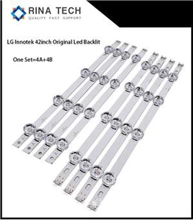
1) Chip package type (on-chip). In this structure, the quantum dot luminescent material replaces the traditional phosphor material and is encapsulated in a patch blue LED, which is also the main packaging method for quantum dots to be used in lighting. This method is applied to the backlight display, and it is also necessary to weld the obtained white light LED of the patch to the LED light bar according to the size of the backlight module. The advantage of this structure is that the amount of quantum dot luminescent material is very small, which reduces the cost. However, this structure has very high requirements on the stability of the quantum dot material.
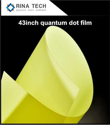
2) Optical film integrated type (on-surface). This structure is mainly suitable for backlighting. The optical film made of quantum dot luminescent material is applied to the backlight module in the form of remote packaging, and the optical film made of quantum dot material is located directly above the light guide plate in the backlight module. In this structure, the large-area preparation cost of the quantum dot optical film is one of the important reasons that limit its large-scale application.
3) Side tube package type (on-edge). This is a compromise between the above two structures. First, the quantum dot material is packaged in a long strip, and then placed on the side of the blue LED light bar and the light guide plate. On the one hand, it can reduce the thermal radiation and light radiation of the blue LED to the quantum dots. The influence of luminescent materials, on the other hand, can also reduce the consumption of quantum dot luminescent materials in practical applications.