Quantum dot LED
Sep 02, 2021
1. What is a quantum dot LED?
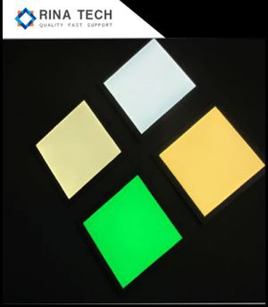
Quantum dot LED is a quantum dot organic light-emitting device with a new structure produced by combining organic materials or LED chips with high-efficiency light-emitting inorganic nanocrystals. Compared with traditional organic phosphors, quantum dots have adjustable luminescence wavelength (covering visible and near-infrared bands), high fluorescence quantum efficiency (can be greater than 90%), small particle size, high color saturation, and low-cost solution processing , High stability and other advantages. It is especially worth noting that the high color purity of the light makes its color gamut can exceed the HDTV standard color triangle. Therefore, light-emitting diodes based on quantum dots are expected to be used in the next generation of flat panel displays and lighting.
Characterize the photoelectric parameters of quantum dots:
1. Photoluminescence spectrum (PL spectrum): The photoluminescence spectrum reflects the relationship between the wavelength of the emitted light and the luminous intensity. From the PL spectrum, basic optical information such as the monochromaticity of the luminescence color, the mechanism of composite luminescence, the particle size and distribution uniformity of the quantum dots, and the intrinsic emission peak wavelength can be obtained. The narrower the half-height width of the quantum dot photoluminescence spectrum, the better the monochromaticity of the light emission of the quantum dot, and the fewer the defects and impurities of the device combined to emit light.
2. Ultraviolet-visible absorption spectrum: The ultraviolet-visible absorption spectrum of quantum dots reflects the degree of absorption of light of different wavelengths by quantum dots. The band gap of quantum dots can be calculated from the position of the absorption peak in the spectrum. The shift between the first absorption peak of the quantum dot absorption spectrum and the emission peak of the photoluminescence spectrum is the Stokes shift. The larger the Stokes shift, the weaker the self-absorption of the quantum dot and the higher the fluorescence intensity of the quantum dot. .
3. Photoluminescence quantum yield: The photoluminescence quantum yield of the quantum dot solution is measured by comparing with the fluorescence intensity of a standard fluorescent substance (generally Rhodamine 6G). The high quantum yield of quantum dots can effectively improve the luminous efficiency of the device, but the quantum yield of pure nuclear quantum dots deposited into a thin film will be 1 to 2 orders of magnitude lower than the quantum yield in solution. Quantum dots also have fluorescence self-quenching phenomenon, which is caused by excitons in quantum dots with uneven size distribution through Foster energy transfer to non-luminescent dots for non-radiative recombination.
Second, the application scheme of quantum dot LED in lighting display
Quantum dots have narrow emission peaks, adjustable emission wavelengths, high fluorescence efficiency, and good color saturation, and are very suitable for luminescent materials for display devices. The application of quantum dot LED in the field of lighting display mainly includes two aspects: a. Quantum dot backlight technology based on the photoluminescence characteristics of quantum dots (QD-BLU, that is, photo-induced quantum dot white LED); b. Quantum-based Quantum dot light-emitting diode technology (QLED) with dot electroluminescence characteristics.
(1) Quantum dot backlight technology
Quantum dot backlight technology, namely photo-induced quantum dot white LED, is a backlight technology based on the photoluminescence characteristics of quantum dots.
(1) Basic principles of quantum dot backlight technology
The principle of quantum dot photoluminescence (PL): the quantum dot layer obtains energy under an external light source, and the electron absorbs the energy of the excited photon to transition from the valence band to the conduction band. The electrons at the bottom of the conduction band and the holes at the top of the valence band can produce band-side recombination luminescence. A part of the electrons and holes are captured by the relatively shallow impurity level, and the electrons and holes captured by the impurity level can directly recombine to produce luminescence. Or transition to deeper defects. Band-edge emission is the main mechanism of device luminescence. The combined luminescence of defects and impurities will affect the luminescence of quantum dots. There are roughly two implementation schemes for pure-color photo-induced quantum dot white light LEDs:
1. Color conversion
The color conversion mechanism is to combine blue LED chips with green and red quantum dots to prepare quantum dot white LEDs. Compared with color mixing to produce white light-appropriately mixing the electroluminescence of quantum dots of various colors, color conversion to produce white light is that the blue light emitted by the LED chip is absorbed by the quantum dots and converted into green light and red light. The RGB principle is combined with the remaining blue light to form white light.
2. Direct white light
The direct white light mechanism means that there is only one kind of light-emitting quantum dot in the light-emitting layer, which is excited by the ultraviolet light emitted by the ultraviolet LED chip to emit light of more than one color, and then directly recombines to produce white light. The mechanism of color mixing and color conversion to generate white light involves the problem of mixing and balancing several colors of light, and the mismatch of each color light will seriously affect the light quality of the white light LED. Therefore, people have a great interest in using phosphors that directly emit white light for solid-state lighting. Since most of the light emission of direct white light quantum dots involves surface defects, the efficiency is low. To realize the ultimate application of direct white light quantum dots, improving the luminous efficiency is the key to research.
(2) Practical application of quantum dot backlight technology
The application of quantum dot backlight technology in practice is to combine blue LED chips with quantum dot materials to replace white LEDs, the background light source of traditional liquid crystal panels. The resulting liquid crystal panels are also called quantum dot LCDs.
There are three ways to encapsulate quantum dots in liquid crystal displays. The first is the "On-Chip" method in which the quantum dot material is directly placed on the blue LED chip. The second is to seal the quantum dots in a thin glass tube. The “On-Edge” method is installed on the LED light entrance port of the backlight light guide plate. The third method is the “On-Edge” method where the sheet material with quantum dots sandwiched between the films is pasted between the light guide plate and the liquid crystal panel. Surface" method.
Source: NANOCO, China Galaxy Securities Research Department
1. The design plan of 3M company in the United States and Nanosys company in Germany
In 2012, 3M and Nanosys jointly developed a quantum dot thickened film (QDEF) made of quantum dot materials that can greatly expand the color gamut of the display. By combining blue LEDs and QDEF, NTSC (National Television Standards Committee) can be easily realized. The wide color gamut with a ratio of 100% achieves the same color expression power as organic EL, while the standard color gamut of the original product is NTSC ratio of 70%.
QDEF disperses quantum dots with diameters of 3nm and 7nm into a thin film, and then clamps the quantum dots through a protective film (two layers of oxygen barrier film). QDEF is attached between the light guide plate of the backlight and the LCD panel ("On-Surface" method), and the backlight source uses blue LEDs to replace the original white LEDs. 3nm quantum dots convert blue light into green light under the irradiation of blue LEDs, while 7nm quantum dots convert blue light into red light under the irradiation of blue LEDs, and mix with part of the blue light that passes through the film to obtain white light. Compared with the original white LED with stable wavelength characteristics, the combination of blue LED and QDEF can produce red, green and blue light sources with sharp peaks, which can effectively improve the color saturation of the LCD. Compared with traditional high color gamut technology, quantum dot technology can increase the color gamut of LCD by 30% without increasing the CF film thickness. On the other hand, it can also increase the brightness of the backlight and save energy.
Source: Nanosys, China Galaxy Securities Research Department
2. Design plan of QDVision company in the United States
QDVision believes that the raw materials of quantum dots can be used in liquid crystal displays with a huge market scale, and promotes "more vivid color" quantum dot LCD TVs. Taking a 42-inch TV as an example, about 100 tons of quantum dot materials are needed every year. In order to cope with the rapid rise of the market, the effective method is to install the quantum dot materials at the entrance of the light guide plate ("On-Edge" method) instead of the light guide plate and the LCD panel. Between ("On-Surface" method), the amount of quantum dot material used in this method is only 1/50 of that when using the On-Surface method, and cheap and stable glass tubes can be used to encapsulate quantum dot materials. Great cost advantage. In addition, although the "On-Chip" method of placing quantum dot materials on the surface of the LED chip can reduce the annual output to one ten thousandth (10kg/year), considering the heat generation of the LED, the "On-Edge" method is the best choice. safe.
At the International Consumer Electronics Show (CES) in January 2013, Sony demonstrated an LCD TV equipped with QDVisions’ quantum dot optical material “ColorIQ”. This LCD TV is named “Triluminos” and the color gamut NTSC ratio is 70% higher than the original one. Increased to 100%, using QDVision's quantum dot technology, can obtain the same color expression power as organic EL.
3. Design plan of British Nanoco
Nanoco, a British supplier of quantum dot materials, has cooperated with Dow Chemical in the field of cadmium-free technology to deploy the quantum dot market. At present, the company's core technology-the production of "CFQD" (cadmium-free quantum dots) that does not contain the toxic element cadmium (Cd) is still limited to a few kilograms per year, which is not enough to meet the growing market centered on LCD panels. need. In order to establish a large-scale production system, the company signed an exclusive licensing agreement with Dow Chemical. The purpose is to use Dow Chemical's production capacity and supply chain in the chemical field to prepare for future market expansion. The technology used by the two partners is an "On-Surface" method in which a sheet material with quantum dots sandwiched between films is pasted between the backlight and the LCD panel. In view of the stability of quantum dot materials and the characteristics of being easily embedded in liquid crystal panels, the On-Surface method is adopted to win the market.
(2) Quantum dot light-emitting diode technology
Quantum dot light-emitting diode technology, QLED technology, is a new type of LED manufacturing technology based on the electroluminescence characteristics of quantum dots, and it is a real quantum dot light-emitting diode. The quantum dot-based backlight technology is essentially a quantum dot LCD, that is, a quantum dot plus liquid crystal panel, which is an improvement of the existing LCD, not a QLED in the true sense.
(1) Basic principles of QLED technology
Quantum dot electroluminescence (EL) principle: QLED electroluminescence is generally attributed to direct carrier injection recombination, Forster resonance energy transfer, or a combination of the two. After electrons and holes are injected, there are two ways to achieve electroluminescence: a. The electrons and holes are directly injected into the same quantum dot to realize radiation recombination luminescence in the quantum dot; b. Inject electrons and holes in organic matter. The holes form excitons, and then transfer energy to the quantum dots in the form of Forster resonance energy transfer. An exciton, an electron-hole pair, is generated in the quantum dot, and finally the electron-hole pair recombines to emit a photon. These two approaches exist at the same time, which can maximize the luminous efficiency of QLEDs.
(2) Four basic structure types of QLED
Since the electro-driven QLED was invented in 1994, the device has undergone four structural developments and changes, and its brightness and external quantum efficiency have been greatly improved.
1. TypeI: use polymer as charge transport layer
This structure uses polymer as the carrier transport layer and is the earliest QLED device structure. Its typical device structure is composed of CdSe pure nuclear quantum dots and polymer double layers or a mixture of the two, sandwiched between two electrodes. This structure uses pure core CdSe with low quantum yield, and there is obvious electroluminescence parasitic in the polymer, so the device has a lower external quantum efficiency (EOE) and a smaller maximum brightness.
2. TypeII: Use organic small molecules as the charge transport layer
In 2002, Coe et al. proposed a Type II QLED device structure combining single-layer quantum dots and double-layer OLEDs, using organic small molecule materials as the carrier transport layer. This structure enables the addition of a single-layer quantum dot layer on the basis of the OLED to separate the carrier transport process and the light-emitting process through the organic layer, thereby improving the external quantum efficiency of the OLED.
Combining the OLED structure with a single layer of quantum dots allows people to see the hope of improving the efficiency of QLEDs. This structured device not only has all the advantages of OLED, but also can improve the spectral purity of the device and realize the tuning of the luminous color. However, the use of an organic layer leads to a decrease in the stability of the device in the air. Like traditional OLEDs, QLEDs with this structure need to be packaged, which increases the production cost and limits flexibility. In addition, the insulation of the organic semiconductor material itself limits the further optimization of the current density of the device, which in turn limits the light-emitting brightness of the device, and the wide light-emitting spectrum of the organic semiconductor material is not conducive to optimizing the color purity of the device.
3. TypeIII: All inorganic carrier transport layer
Compared with the TypeII structure type, this structure type replaces the organic carrier transport layer with an inorganic carrier transport layer. This greatly improves the stability of the device in the air and enables the device to withstand higher current densities. Caruge et al. used the sputtering method to prepare an all-inorganic QLED with zinc tin oxide and nickel oxide as the electron and hole transport layers, respectively. The maximum current density that the device can withstand reaches 4Acm-2, but the external quantum efficiency is less than 0.1 %. The low device efficiency is attributed to the destruction of the quantum dots during the sputtering of the oxide layer, the imbalance of carrier injection, and the quenching of the quantum dot fluorescence generated when the quantum dots are surrounded by conductive metal oxides.
4. TypeIV: The organic hole transport layer is mixed with the inorganic electron transport layer
The TypeIV structure type uses organic and inorganic mixed carrier transport layers to make QLED devices. The structure generally uses N-type inorganic metal oxide semiconductors as the electron transport layer and P-type organic semiconductors as the hole transport layer. The QLED of the hybrid structure has high external quantum efficiency and high brightness at the same time. Among them, Qian et al. reported that the external quantum efficiency is 1.7%, 1.8%, 0.22%, and the maximum brightness is 31000cdm-2, 68000cdm-2, 4200cdm-2 red, green, and blue mixed structure QLED.
Recently, a 4-inch QD-LED color display has been developed using the Type IV hybrid structure. Using micro-contact printing technology, the resolution of the solubilized QLED color display reaches 1000 ppi (pixel size is 25 μm).
Compared with the TypeII structure type, the quantum dot film thickness used in the TypeIII and TypeIV structure types exceeds a single layer to 50nm. Therefore, the working mechanism of the TypeIV structure type focuses on the carrier injection mechanism rather than the Forster energy transfer mechanism.
(3) Preparation method of QLED device
In the preparation method of QLED devices, the preparation technologies that have been successfully proven include phase separation technology, inkjet technology and transfer technology.
1. Phase separation technology
The phase separation technology can prepare large-area ordered colloidal monolayer quantum dots well. The quantum dot film can be prepared from a quantum dot mixed solution of organic aromatic material and aliphatic material by using a spin coating method. During solvent drying, the two different materials are separated to form a desired single-layer quantum dot on the surface of the organic semiconductor. This method is reliable, flexible, and can be precisely controlled at the same time with good repeatability. The solution concentration, solution ratio, quantum dot size distribution, and the shape of the quantum dots all affect the structure of the film. Controlling these factors well can obtain QLEDs with high efficiency and high color saturation. However, because this method uses spin coating, it can only produce monochromatic display screens.
2. Inkjet technology
For full-color displays, it is hoped to find a preparation process that can produce a single-layer quantum dot pattern without placing more requirements on materials and device structures. The inkjet process is a preparation technology that meets these conditions. Inkjet technology is to use micron-level print nozzles to spray the prepared "ink" with special functions on the
Pixel units are formed on the patterned ITO substrate. The use of the spray method can accurately control the amount and position of the on-demand distribution, which can reduce the production cost, and can also realize a large area and large size display.
3. Transfer technology
The transfer technology is to first coat the quantum dot solution on the silicon plate, then evaporate, and then press the protruding part into a quantum dot layer, remove the surface layer and transfer it to a glass substrate or a plastic substrate. This process achieves the most sub-point Transfer to the substrate.
(4) The main problems of current QLED
1. Preparation cost
The manufacturing cost of QLED devices can be roughly divided into the cost of raw materials and the manufacturing cost of processing these materials. Since QLEDs currently use similar toolbox thin film processing technologies, such as inkjet and micro-contact printing, thermal evaporation quantification and sputtering, etc., although QLEDs have a much lower cost than OLEDs in terms of structure and manufacturing technology, they require a high-demand manufacturing environment. There is still some distance between it and commercialization.
2. Service life
At present, the lifespan of QLED devices at the lowest video brightness (100cd/m2) is only 100-1000 hours, which is far less than the lifespan required by the display (more than 10,000 hours). Due to the lack of in-depth theoretical research at present, there may be many factors that cause the short life of the device. As QLED devices evolved on the basis of OLEDs to a certain extent, the inherent instability of organic matter as the charge transport layer of QLEDs may be a reason for their short device life. On this basis, improving the stability of the organic matter in the device has become a research direction to increase the lifespan of QLEDs.
Third, the application of quantum dot LED
Quantum dot LEDs mainly have two application directions: one is a quantum dot LCD using quantum dot backlight technology, and the other is a quantum dot light-emitting diode QLED. In these two application directions, the application of quantum dot LCD is relatively simple and mature, and quite a few products have appeared, while QLED is still in continuous development and improvement.
(1) Application advantages of quantum dot LED
Since quantum dot LEDs use quantum dot materials, they naturally have many advantages over organic fluorescent materials.
(2) Overview of the development of quantum dot LED applications
(1) In 2010
LG demonstrated a new type of panel at the SID International Display Information Conference. The panel uses quantum dot LEDs as its background light source. The color purity of the LCD panel will be further improved, thereby expanding the display color gamut of the panel by 30%.
(2) 2011
NanoPhotonica, a developer of advanced materials, has made a major and feasible breakthrough in quantum dot LED display technology, which will soon be used in mass production of displays. Displays produced with NanoPhotonica-QLED technology will have better picture quality, while power consumption will be reduced by 30%, price will be reduced by 75%, and service life will be doubled. It has a wide range of uses and can be used in displays of various sizes. Behind the wide range of uses is the cost-effective inkjet printing technology that does not require vacuum evaporation.
Samsung Electronics uses the organic layer and the inorganic layer as the electron and hole transport layers of the quantum dot light-emitting layer, respectively, to fabricate quantum dot light-emitting diodes. By patterning the quantum dot film by the transfer method, Samsung Electronics has produced a prototype of a 4-inch full-color active matrix QLED display device.
QDVision demonstrated a 4-inch full-color quantum dot LED display on SID. The image quality and efficiency of the display have reached the level of existing OLEDs. QDVision expects to achieve mass production of quantum dot LED displays within 3-5 years.
Nanosys demonstrated a quantum dot enhancement film QDEF technology at SID in 2011. This technology adds a quantum dot enhancement film between the backlight unit of the LCD display and the display module, which can increase the color gamut of the existing LCD display by 50%. %, reaching the color gamut level with OLED.
In 2011, Nanosys developed a 47-inch full HD LCD TV with a color gamut of 80% NTSC using blue LED excitation quantum dot light-emitting film as a background light source.
(3) 2013
In June 2013, Sony launched a high-end LCD TV model that uses quantum dot technology in the backlight. In October of the same year, Amazon launched a tablet computer that uses quantum dots in the LCD backlight.
(4) 2014
In April, the VX2457sml of ViewSonic, a leading global technology brand in the United States, is a representative of quantum dot technology. With quantum dot display technology, the number of colors that can be displayed can be further increased, and the display color gamut of the panel can be increased to 99% AdobeRGB, LCD The color purity of the panel has also been greatly improved, and the image quality has been improved, thereby presenting users with a professional and extremely realistic color display.
In September, Samsung Electronics, LGE and TCL all exhibited LCD TVs using quantum dot backlight technology for the first time at the International Consumer Electronics Show (IFA) in Berlin. Among them, Samsung Electronics will mass-produce QDLCD TVs in the first quarter of next year. SDC will provide Opencell. The first batch of products will be 55 inches and 66 inches in size, and will be positioned in the ultra-high-end market.
TCL will use the Huaxing 55-inch UHD panel and 3MQDEF, with a color gamut of 105%, and plans to mass-produce it as early as the end of 2014. LGE has also been cooperating with QDvision to develop quantum dot backlight technology and plans to launch QDLCD TVs, but its product strategy in 2015 will still focus on OLED products. Sony also has plans to launch QDLCD TV products over 55 inches.
In early 2014, the United States Patent and Trademark Office approved a patent called "Quantum Dot Enhanced Display with Dichroic Filter" filed by Apple in 2012. The patent details the quantum dot technology and how this technology is applied in On a mobile device like the iPhone.
(5) 2015
Samsung vigorously promoted the new "SUHDTV" series at the CES2015 Electronics Show, highlighting its advantages in brightness, color reproduction, and detail presentation, which are also different from ordinary UHD (Ultra HD) TVs. But in essence, SUHD is also based on quantum dot technology, but Samsung has optimized the nanocrystal and image processing engine, which looks better than the previous 4KLED backlight TV.
At CES2015, TCL Group also held a new product promotion conference at the exhibition, and released China's first quantum dot TV H9700 for the North American market, which became a highlight of the 2015 CES exhibition in the United States.
(6) 2016
At the 2016 IFA exhibition, Samsung showcased a variety of new large-screen TVs. Quantum dot TVs based on SUHD have unsurprisingly occupied half the sky-in addition to 19 new quantum dot TVs covering 43 inches to 88 inches, Samsung also Released the first quantum dot curved gaming display.
In September, TCL launched an important autumn product line, launching the high-end sub-brand "Chuangyi" (English name "Xess"), and its quantum dot TV, tablet computer, mobile phone and other terminal products, of which the quantum dot TV X2 is used as Important flagship products are expected to be officially launched on the market in three months.
(3) Quantum dot LED application market analysis
The application market of quantum dot LEDs is divided into QLED and quantum dot LCD. Since the commercialization of QLED is not mature enough, the current quantum dot LED application market is basically occupied by quantum dot LCD.
(1) Global QLED application market forecast
Although all eyes are now on the quantum dot LCD, QLED is the real quantum dot light-emitting diode, which is expected to become the next generation of OLED display technology. According to the forward-looking forecast of IDTechExResearch, the market size of QLED can reach 11.2 billion U.S. dollars by 2026, and the market size of the display field is 9.6 billion U.S. dollars, accounting for about 85%.
Figure 26: QLED application market scale forecast
(2) Global Quantum Dot LCD Application Market Forecast
Quantum dot display technology has been around since the 1990s, but it has only recently become popular in the TV market. LCD panels have been developed for decades, and the main improvement lies in the development of backlight technology. LED backlights have now become the mainstream and have better display effects than traditional cold cathode fluorescent lamp backlights. But obviously LED backlight is not a panacea. The so-called "WhiteLED" has a very wide spectrum. Therefore, in order to display more saturated red, green, and blue colors, more precise dimming technology is required, and there are also some bottlenecks. The self-luminous OLED has better color reproduction effect, but the cost is very high, the market acceptance is low, and mass production on a large scale is very unrealistic. Quantum dots are a more efficient display technology in liquid crystal display technology. Quantum dots can convert pure blue light sources into red and green, suppress color cast, and achieve a more balanced output of the three primary colors. At the same time, its power consumption and cost are also lower than OLED. Considering that quantum dot technology can bring higher energy efficiency and color performance, while also reducing costs, quantum dot LCD may soon become the most popular choice in the high-end TV market.
The market size of quantum dot LCD in 2015 was 77.6 million US dollars, and it is expected that the market size will reach 477 million US dollars by 2020, a year-on-year increase of 515%. It can be seen that the market size of quantum dot LCDs will show explosive growth in the next five years, with huge potential.
Figure 27: Quantum LCD market size forecast
Quantum dot LCD has three packaging forms: On-Surface, On-Edge and On-Chip. Currently, the first two methods are the main packaging forms of quantum dot LCD. In 2015, the market size of quantum dot LCD packaged in On-Surface form and On-Edge form was US$69.5 million and US$8.1 million, respectively, and the market size is expected to be US$425.4 million and US$16.1 million by 2020, respectively. The market size of the On-Surface format is increasing year by year, and the market size of the On-Edge format in 2018 is expected to reach 20.2 million U.S. dollars, followed by a downward trend. The quantum LCD packaged in On-Chip format is expected to have a market size of 7 million U.S. dollars in 2018 and reach 3570 U.S. dollars in 2020, which will exceed the market size of On-Edge format package. On-surface packaging is the mainstream choice for quantum dot LCDs. The market share in 2015 was 89.6%, and it is expected to account for 89.1% in 2020.
Due to its excellent performance, quantum LCD will be widely used in television display (TV), monitoring display (monitor), notebook computer display (notebook), tablet computer display (tablet) and mobile phone display (smartphone). In 2015, the market size for TV, monitor and tablet was 73.5 million US dollars, 3.5 million US dollars and 500,000 US dollars, respectively, and the shipments were 1.4 million, 400,000 and 100,000 units, respectively. The market sizes are expected to be respectively by 2020 For 41.3 million US dollars, 24.2 million US dollars and 19.3 million US dollars, shipments were 24.5 million units, 3.2 million units and 4.7 million units. In 2016, the market size of notebooks was 700,000 U.S. dollars, with shipments of 100,000 units. It is estimated that by 2020, the market size will be 4 million U.S. dollars, with shipments of 800,000 units. The market size for smartphones in 2018 was 1.1 million U.S. dollars, with shipments of 500,000 units. It is estimated that by 2020, the market size will be 13.5 million U.S. dollars, with shipments of 7.4 million units. Quantum dot TV is the main application field of quantum dot LCD, accounting for about 94.8% of the total market in 2015, and it is expected to be about 87.2% in 2020.
Figure 31: Shipment forecast for quantum dot LCD applications
In the next five years, quantum dot TVs will occupy most of the market for quantum dot LCD applications. In 2015, the shipments of 40-49-inch quantum dot TVs were 100,000 units, 50-59 inches were 800,000 units, and 60-69 inches were shipped. The inch is 400,000 units, and shipments by 2020 are expected to reach 8.3 million units, 11.9 million units and 3.9 million units respectively. It is estimated that the shipment of quantum dot TVs larger than 70 inches will be 100,000 units in 2017 and 400,000 units by 2020. 40-60 inches is the mainstream demand for quantum dot TVs, accounting for 69.2% of total shipments in 2015 and 82.5% in 2020. In contrast, the demand for more than 70 inches is small.
Figure 33: Shipment forecast of different sizes of quantum dot TVs
4. Major global quantum dot manufacturers
At present, there are about 60 units in the world conducting quantum dot research, including enterprises, universities, research institutions, etc. Among them, the three world’s leading manufacturers of quantum dot materials-Nanoco in the United Kingdom, QDVision in the United States and Nanosys in Germany, have gradually Forming a three-legged situation, these three companies have almost divided up the market, and Hangzhou Nanojing Technology Co., Ltd. is the only domestic enterprise with quantum dot technology research and development capabilities.
(1) Major foreign quantum dot companies
(1) Nanoco, UK
The British Nanoco was established in 2001, and its market position is to be a manufacturer and supplier of environmentally friendly cadmium-free quantum dots (CFQD). It cooperated with Dow Chemical in the United States to trial-produce liquid crystal displays using cadmium-free (Cd) quantum dots in 2014 It was demonstrated during "SID2014" on June 2 and adopted the "On-Surface" package form, but there have been no public reports on the application products. In addition, Samsung’s upcoming mass production of quantum dot backlight materials mainly come from Nanoco and Dow Chemical. The company's current market capitalization is $196 million.
Nanoco's operating income and net profit in 2015 were 3.2 million U.S. dollars and 12.9 million U.S. dollars, respectively. For six consecutive years, the net profit was negative and expanding, and it was at a loss. Its operating income in 2015 came from three parts: royalty and license income, quantum dot materials and technical services, of which quantum dot materials accounted for 21.9% of its operating income.
Nanoco quantum dot materials business overview:
1. Backlight display: CFQD can significantly increase the display color gamut (increase by 30%) to make the image more lifelike, the color is more beautiful, and there is no need to change the existing LCD and LED display process mode, the cost is lower, and it is easier to be used by the majority of LCD (LED ) Accepted by the manufacturer. Application direction: mobile phone panel, tablet computer, computer display, TV, etc.
2. Lighting: By controlling the size of the CFQD, the color temperature and color rendering index of the light can be accurately adjusted, so as to meet the individual needs of customers for light. In addition, due to the more excellent photoelectric conversion efficiency of CFQD, the use of LED light sources can be reduced to achieve more energy-saving purposes. Application direction: LED packaging, LED lighting devices, LED lamps, LED lighting products, etc.
3. Thin film solar energy: Nanoparticles (CIGS) produced by Nanoco have very good photoelectric conversion efficiency. Different from the current processing methods, the nanoparticles can be used to produce thin film solar cells by the solution method, and the material utilization rate reaches 90%, which is much higher than The current evaporation method and sputtering
Shooting method
4. Biomedicine: water-soluble CFQD and functional CFQD, application directions: bioimaging, in vivo and in vitro in vivo diagnosis.
(2) QDVision, USA
The United States QDVision was founded in 2004 by researchers from the world-renowned Massachusetts Institute of Technology (MIT), including Moungi Bawendi, the father of quantum dot display technology. In addition to owning more than 250 patents and pending patents, it has also obtained approvals from the United States. Many awards including the famous "Presidential Green Chemistry Award" issued by the Environmental Protection Agency. It cooperated with Nexxus Lighting of the United States to launch a commercial quantum dot lighting source in 2009. The quantum dot backlight tube released in 2013 was applied to the TV set of Sony Corporation in Japan, using the "On-Edge" packaging method. QDVision claims that its monthly output of quantum dot optical components can reach 1 million.
QDVision is a leader in the field of quantum dot display technology. Its ColorIQ quantum dot display technology provides a unique component solution that enables the display to output "full gamut" colors. Since 2013, the company has sold more than one million ColorIQ optical devices and continues to cooperate with brands in the TV and display market including TCL, Hisense, Philips and Konka. Quantum dot TVs and displays using ColorIQ technology have It is listed in China, Japan and Europe.
ColorIQ quantum dot display technology is an advanced light-emitting semiconductor technology developed by QDVision. Related products are made of quantum dot materials, which can emit very pure and saturated narrow bandwidth red, green, and blue light. Through the integration of ColorIQ optical components and The customer’s display technology, LCD TVs can achieve a wider color gamut and 100% NTSC standard. Application direction: large-screen LCD TV, personal computer, workstation monitor, smart phone, lighting field, etc.
(3) Nanosys, Germany
German Nanosys was founded in 2001 and is one of the leaders in quantum dot display technology. The company holds more than 300 quantum dot display related patents. In 2012, it cooperated with 3M to develop quantum dot thick film (QDEF) technology. , The use of QDEF technology can not only expand the color gamut from 70% of NTSC to 100%, but also increase the luminous efficiency expressed by the ratio of the brightness of the LCD panel to the power of the backlight by about 50%. It adopts the "On-Surface" Package form.
Nanosys’ quantum dot materials business mainly includes quantum dot concentrates and QDEF technology. The company currently has the world’s largest production base for quantum dot concentrates with an annual output of 25 tons and an annual supply of 6 million 60-inch quantum dot TVs.
With the ability of sub-dot materials, a series of new quantum dot products, such as quantum dot pipes, will be launched after 2015. The company has established close cooperation with some well-known computer and monitor brands such as 3M, Samsung, Sharp and LG, and its products are widely used in tablet computers, TVs, smart phones, etc.
(2) Major domestic quantum dot companies
(1) Hangzhou Najing Technology Co., Ltd.
Najing Technology was established in August 2009. It is a national high-tech enterprise with quantum dot semiconductor new materials as its core technology. Its main business is the research, manufacturing and application technology and product development of quantum dot new materials. Dot material's design, synthesis and surface modification are in a leading position in the world, and it is the only domestic company listed on the New Third Board. It has strong scientific research capabilities and its current market value is 1.63 billion yuan.
The operating income and net profit of Najing Technology in 2015 were 7.31 million yuan and -4.9 million yuan, respectively. The net profit for four consecutive years was negative, but the losses in the past three years have been decreasing. The company's quantum dot materials and their applications are in the market introduction and verification period. Although it has irreplaceable technological competitive advantages, and its application products including quantum tubes have begun mass production, there are still continuing losses before objective operating income is formed. Operational risk. Its operating income in 2015 came from five parts: lighting products, semiconductor luminescent materials, technical services, biological products and display products. Operating income accounted for 56.8%, 26.2%, 11.4%, 4.7% and 1%, respectively. Display products The proportion is small.
Overview of Najing Technology's main business:
1. Quantum dot materials: divided into four product systems-cadmium-containing quantum dot reagents, cadmium-free quantum dot reagents, metal nanocrystals and oxide nanocrystals, which are widely used in light-emitting devices, solar cells, catalysis, biomarkers and biomedicine Basic research and application development in other fields.
2. ColorIn quantum dot display technology: Products include quantum dot light conversion devices (Q-LCD) and quantum dot light conversion films (QLCF), which are widely used in terminal products such as TVs, monitors, and mobile phones.
3. QLED: The OLED printing and display project research center has been established, and the industrial development of QLED printing and display technology is being actively promoted.
4. Biomedicine: Established a wholly-owned subsidiary, Beijing Najing Biotechnology Co., Ltd., dedicated to the application and promotion of quantum dots in the field of life sciences. Products include quantum dot markers, quantum dot labeling kits, quantum dot quick inspection platforms, etc. .
5. Nano crystal natural light: Using the exclusive quantum dot nano crystal combined with the CREE global authorized remote excitation technology of the United States, a 3D silicone spherical mask light-emitting device based on natural light spectrum simulation technology is developed, which overlaps more than 95% of the natural light and healthy visible spectrum area. It is by far the closest artificial light source to natural light.